Turn on suggestions
Auto-suggest helps you quickly narrow down your search results by suggesting possible matches as you type.
Showing results for
- Republic of Gamers Forum
- Discussions
- Overclocking & Tweaking
- Radeon HD 6870 PCB and GPU Pictured
Options
- Subscribe to RSS Feed
- Mark Topic as New
- Mark Topic as Read
- Float this Topic for Current User
- Bookmark
- Subscribe
- Mute
- Printer Friendly Page
Radeon HD 6870 PCB and GPU Pictured
Options
- Mark as New
- Bookmark
- Subscribe
- Mute
- Subscribe to RSS Feed
- Permalink
10-15-2010
05:44 PM
- last edited on
03-05-2024
06:45 PM
by
![]() ROGBot
ROGBot
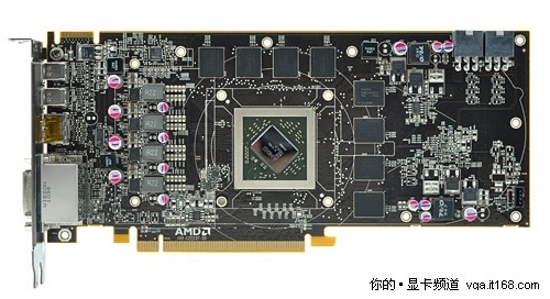
The fine folks at IT168 revealed the first pictures of the Radeon HD 6870 PCB with its cooler completely off, and in its production livery (black). Also let out is the first [clear] picture of the GPU itself. The PCB was first pictured in its nascent qualification sample form, with a development GPU cooler on. The final version of the PCB sticks to its qualification sample for the most part, it has VRM components positioned forwards, trailed by the GPU and its memory. The card makes use of a 4+1+1 phase VRM. All eight memory chips are on the obverse side, each with its own 32-bit wide path, since there's a 256-bit memory interface.
The GPU package is of the same dimensions as the Cypress package, albeit a smaller die. We're getting to hear that Barts is pin-compatible with Cypress (meaning that a Barts GPU can be placed onto a Cypress PCB, given the appropriate BIOS, and it will work), however, no AIB is likely to reuse Cypress PCBs other than for Eyefinity6 designs, because while Barts can make do with a 6-layer PCB, close to every existing Cypress PCB is an 8-layer one, and that Cypress PCBs lack the second mini-DP connector. The die is placed diagonally on the package (à la Cypress and R600), it is rectangular, while the Cypress die is more or less square. ChipHell.com contributor musicinlove did a nice size measurement and comparison. Finally, the AMD "arrow" logo is etched onto the die, it's curtains down for ATI.

Source: http://www.techpowerup.com/132802/Radeon-HD-6870-PCB-and-GPU-Pictured.html
Labels:
- Labels:
-
Overclocking
-
Tuning
-
Tweaking
5,374 Views
0 REPLIES 0
Related Content
- [Resolved]asus crosshair v formula z bios screen not displaying correctly in Promotions & General Discussions
- AMD Firepro W8100: It's designed for PCIE 3.0, but my MB is only 2.0. Problem? in Overclocking & Tweaking
- Computer won't wake on after hibernation "sleep" without power drain off/on tweek!?! in Overclocking & Tweaking
- Hero + 4670k - any% OC Fails in Overclocking & Tweaking
- Crosshair V formula-z wont post, FF error code on MB. (just upgraded to watercooling) in Overclocking & Tweaking
