ASUS Crosshair V Formula BIOS Guide – Overclocking
[video]http://www.youtube.com/watch?v=j3FmXDbUxBo[/video]

AMD’s 9 series chipset gets UEFI BIOS Upon entering UEFI BIOS, you’ll need to head over to the AI Tweaker section to embark on any overclocking: Load Extreme OC Profile: Contains pre-set BIOS profiles to help overclock the system if you don’t wish to experiment with settings yourself. The profiles used are general fine for normal use, though may set certain voltages a little higher than absolutely necessary simply to ensure that the profiles work with a wide range of processors and memory. If you don’t plan on spending copious level of time in the BIOS fiddling with various parameters, then these profiles will help you overclock the system with minimal fuss. OC Tuner: Our automated routine that overclocks a system based upon cooling and components. When selected the system will run a series of tests during system boot (do not be alarmed if your system reboots a few times after selecting this setting and saving and exiting BIOS – that’s normal). After the procedure is complete, you may wish to enter the operating system and run your preferred stability tests to confirm stable operation. Do bear in mind though that for compatibility purposes OC Tuner will use memory module JEDEC timing values. CPU Ratio: Sets the CPU core multiplier ratio, which is multiplied by the “CPU Bus/PEG Frequency” setting to obtain CPU core frequency. The current and target processor speeds are shown in the top-left of the AI Tweaker menu. AMD Turbo Core Technology: Sets the Turbo multiplier ratio. Turbo Core Technology allows the processor to ramp its core frequency to a higher level during software loading provided that the thermal design power ratings are not breached (by default). This setting can be used to over-ride the default Turbo Core multiplier ratio (TDP permitting). The multiplier values available for this function are dependent upon the processor used. If using a manual setting that is higher than the default Turbo Ratio, care must be taken to ensure that processor core voltage is adequate enough to sustain Turbo Core frequency speeds. *To be Updated at a later date * CPU Bus/PEG Frequency: Sets the reference clock frequency from which the processor, memory, memory controller and the HT bus are derived. Adjusting this value allows granular control over these bus frequencies which can then be offset using multiplier control of each corresponding bus to ensure that the functional limitations of a bus are not breached while overclocking the system. PCIe Frequency: Directly sets the PCIe bus operating frequency. Manipulation of this setting is not required for most overclocking. Memory Frequency: Sets the memory bus multiplier ratio and is used in conjunction with the value entered in the CPU/Peg Frequency setting to obtain the memory operating frequency. The range of available multipliers ratios depends upon the processor used while usage is dependant on the operational limitations of the processor and memory modules. CPU/NB Frequency: Sets the multiplier ratio of the integrated memory controller (on the processor die) and is used in conjunction with the value entered in the CPU/Peg Frequency setting to obtain the memory controller operating frequency. The range of available multipliers ratios depends upon the processor used while usage is dependent on the operational limitations of the processor. HT Link Speed: Sets the multiplier ratio of the HT bus and is used in conjunction with the value entered in the CPU/Peg Frequency setting to obtain HT link operating frequency. The range of available multipliers ratios depends upon the processor used (and which CPU/NB Frequency ratio is used) while usage is dependent on the operational limitations of the processor and motherboard.

CPU Spread Spectrum: Modulates the processor clock to reduce radiated noise emissions – disable for overclocking as clock modulation reduces logic sampling margins. PCIe Spread Spectrum: Modulates the PCIe clock to reduce radiated noise emissions – disable for overclocking as clock modulation reduces logic sampling margins. EPU Power Saving Mode: Sets the load dependant phase switching conditions; the VRM is made up of multiple phases (each phase has at least two FETs). During light-load conditions FETs can be switched off to save power – setting EPU to Enabled allows this to happen. If EPU is disabled all phases will remain on, regardless of system loading. DRAM Timing Control: Takes us to the DRAM timing sub-menu, where primary, secondary and tertiary memory timings can be set.

These timings will automatically be offset according to memory module SPD and memory frequency. Should you wish to experiment with various timings, the primary settings are the most important for overall memory performance. Most timings are set in DRAM clock cycles, hence a lower value results in a more aggressive setting (unless otherwise stated). As always, performance increases from memory tuning are marginal and are generally only noticeable during synthetic benchmarks. Either way, voltage adjustments to VDIMM, CPU/NB voltage and to a lesser extent CPU Core Voltage may be necessary to facilitate tighter timings. DRAM CAS Latency: Column Address Strobe defines the time it takes for data to be ready for burst after a read command is issued. As CAS factors in every read transaction, it is the most important timing in relation to memory read performance. To calculate the actual time period denoted by the number of clock cycles set for CAS we can use the following formula: tCAS in Nano seconds=(CAS*2000)/Memory Frequency This same formula can be applied to all memory timings that are set in DRAM clock cycles. DRAM RAS TO CAS Latency: Also known as tRCD. Defines the time it takes to complete a row access after an activate command is issued to a rank of memory. This timing is of secondary importance behind CAS as memory is divided into rows and columns (each row contains 1024 column addresses). Once a row has been accessed, multiple CAS requests can be sent to the row the read or write data. While a row is “open” it is referred to as an open page. Up to eight pages can be open at any one time on a rank (a rank is one side of a memory module) of memory. DRAM RAS# PRE Time: Also known as tRP. Defines the number of DRAM clock cycles it takes to precharge a row after a page close command is issued in preparation for the next row access to the same physical bank. As multiple pages can be open on a rank before a page close command is issued the impact of tRP towards memory performance is not as prevalent as CAS or tRCD - although the impact does increase if multiple page open and close requests are sent to the same memory IC and to a lesser extent rank (there are 8 physical ICs per rank and only one page can be open per IC at a time, making up the total of 8 open pages per rank simultaneously). DRAM RAS Active Time: Also known as tRAS. This setting defines the number of DRAM cycles that elapse before a precharge command can be issued. The minimum clock cycles tRAS should be set to is the sum of CAS+tRCD+tRTP. DRAM READ to PRE Time: Also known as tRTP. Specifies the spacing between the issuing of a read command and tRP (precharge) when a read is followed by a page close request. The minimum possible spacing is limited by DDR3 burst length which is 4 DRAM clocks. Most 2GB memory modules will operate fine with a setting of 4~6 clocks up to speeds of DDR3-1866 (depending upon the number of DIMMs used in tandem). High performance 4GB DIMMs (DDR3-2000+) can handle a setting of 5 clocks provided you are running 8GB of memory in total and that the processor memory controller is capable. If running more than 8GB expect to relax tRTP as memory frequency is increased. DRAM RAS to RAS Delay: Also known as tRRD (activate to activate delay). Specifies the number of DRAM clock cycles between consecutive Activate (ACT) commands to different banks of memory on the same physical rank. The minimum spacing allowed at the chipset level is 4 DRAM clocks. A setting of 5 clocks and upwards may be necessary to achieve stability at speeds over DDR3-1866. DRAM Write to Read Delay: Also known as tWTR. Sets the number of DRAM clocks to wait before issuing a read command after a write command. The minimum spacing is 4 clocks. As with tRTP this value may need to be increased according to memory density and memory frequency. DRAM CAS Write Latency: Also known as CWL. Sets the column write latency timing for write operations to DRAM. For absolute stability the minimum value should be set equal to read CAS, as the timing constraints of accessing a column are the same, although there are some modules that can handle a setting of Read CAS -1 or Read CAS -2 depending upon memory frequency . This timing is just as important as read CAS because data has to be written to DIMMs in order to be read. DRAM Write Recovery Time: Defines the number of clock cycles that must elapse between a memory write operation and a Precharge command. Most DRAM configurations will operate with a setting of 10 clocks up to DDR3-1866. After that, relaxing to 12+ clocks may be necessary at DDR3-2000+. DRAM Ref Cycle Time: Also known as tRFC. Specifies the number of DRAM clocks that must elapse before a command can be issued to the DIMMs after a DRAM cell refresh. DRAM Row Cycle Time: Also known as tRC. Stipulates the number of DRAM clocks that must elapse before another Activate Command (row select) to the same bank. The minimum spacing is tRAS+tRP. Setting a higher value may aid stability somewhat at the chance of a very small performance hit. DRAM READ to WRITE Delay: Sets the read to write delay timing where the write follows a read on the same rank. A setting of 4 clocks should suffice for most configurations, although some DIMMs may need a higher setting to aid stability as memory frequency is increased past DDR3-1866 at the expense of performance. DRAM WRITE to READ Delay (DD): Sets the delay period between a write command that is followed by a read command; where the read command requires the access of data from a different DIMM. A value of 1 clock is possible on high performance memory. For higher density modules this value may need relaxing to 2~4 clocks as memory frequency is increased.

DRAM WRITE to WRITE Delay: Sets the delay between two consecutive write commands. The BIOS does not stipulate if this is a different rank or different DIMM timing. A setting of 4 clocks works with most configurations, but may need relaxing to 5~7 clocks if 16GB memory configurations are used or if 8GB configurations are used at speeds in excess of DDR3-2000. DRAM READ to READ Delay: Sets the delay between two consecutive read commands. The BIOS does not stipulate if this is a different rank or different DIMM timing. A setting of 4 clocks works with most configurations, but may need relaxing to 5~7 clocks if 16GB memory configurations are used or if 8GB configurations are used at speeds in excess of DDR3-2000. DRAM Refresh Rate: Also known as tREFI. Sets the delay period before a DRAM refresh command is issued to all ranks. A higher number is more aggressive as it sets a longer delay period between refresh commands. 4GB configurations should operate fine with a setting of 7.8us, 8 and 16GB configurations may need a setting of 3.9us if overclocking past DDR3-2000 and DDR3-1600 respectively. DRAM Command Rate: Specifies the number of DRAM clock cycles that elapse between issuing commands to the DIMMs after a chip select. The impact of Command Rate on performance can vary. For example, if most of the data requested by the CPU is in the same row, the impact of Command Rate becomes negligible. If however the banks in a rank have no open pages, and multiple banks need to be opened on that rank or across ranks, the impact of Command Rate increases. Most DRAM module densities will operate fine with a 1N Command Rate. Memory modules containing older DRAM IC types may however need a 2N Command Rate.
DRAM Driving Control: Takes us to the Drive Strength sub-menu (shown later in the guide). GPU.DIMM Post: opens a sub-page which shows how many GPUs are inserted into the PCIe slots and how many DIMMs are being used. If there are any peripheral issues or system bus speeds have been increased too far, one of the GPUs or memory modules may not show in the GPU DIMM Post screen – a quick glance here can save a lot of head-scratching. On this platform however, checking the Performance Tab of Task Manager to check if all DIMMs are mapped is also advised when pushing DRAM past DDR3-2000. Digi+ VRM/POWER Control: Takes us to the power control sub-menu (shown later in the guide).

Drive strengths shown are for Corsair Dominator GT DDR3-2200 8-8-8-24 Rev 2.1 (Elpida Hyper). These settings only need adjusting at high memory operating frequencies and/or for benchmarking purposes when chasing every last MHz. Not all memory modules will respond to drive strength adjustments as there are sometimes issues related to timing mismatches that cannot be corrected by changing drive strengths. Signal line reflections due to impedance mismatches can cause instability at high operating frequencies. Drive strength setting manipulation increases or decreases buffer output current on the associated signal lines and may help increase bus clocking margins when setup correctly. It is imperative that we change only one setting at a time (for both channels), monitor for changes and then make further adjustments. Do not change any other overlcocking related settings or voltages in unison with drive strength adjustments. Voltage and bus adjustments should only be made after assessing the impact of a change to any of the parameters in the drive strength setting menu. Use HCI Memtest first to assess changes in failure times to gauge the impact on stability before moving on to Prime95 or Linpack. Time spent on Memtest will reduce drive strength change requirements during higher levels of bus IO. Once Memtest is stable, a change of only one~two steps may be needed to obtain full memory module and memory controller stability. CKE drive strength: Sets the drive strength for clock enable signals. This line doesn’t transition as much as the other lines, however, that is not to say that this setting is not important. GSkill Flare 4GB DIMMs prefer a manual setting of 1.5X, while Corsair 2.1 revision Hyper prefer 1X. An incorrect value for CKE Drive Strength will result in a non-POST. CS/ODT: Chip Select/On Die Termination drive strength, sets the output buffer impedance for chip select signal lines and termination drive strength. 4GB DIMMs may benefit from a setting of 1.5X over DDR3-2000. For Elpida Hyper try 1X. ADDR/CMD Drive Strength: Sets the output buffer impedance for Address and Command signal lines. A setting of 1.25X is preferred by GSkill Flare DDR3-2000 4GB modules. For Elpida Hyper based modules try 1X. MEMCLK Drive Strength: A setting of 1.5X suits most modules and is the default setting – change only after experimenting with all other drive strength settings first. DATA Drive Strength: Sets the buffer drive strength for the DQ lines. A setting of 1.25X is preferred by GSkill Flare 4GB modules. For Elpida Hyper try 1X. DQS Drive Strength: Sets the buffer drive strength of the DQS lines. At high memory frequency try a setting of 0.75X on GSKill Flare and Elpida Hyper. Other Elpida die favor 1X~1.25X Processor ODT: Sets on die termination resistance of the processor transceiver stages – can be left on AUTO under all normal operating conditions.

CPU Load Line Calibration: The “Regular” option sets a margin between the user set voltage and the actual voltage to ensure that the real-time voltage level does not breach (overshoot) the set VID by longer than AMD specifications. Medium and High, set a tighter margin between the idle and full load voltage, so that idle voltage does not need to be ramped excessively to meet full-load voltage requirements when the processor is overclocked. Ultra-High and Extreme may over-volt past what you’ve set in BIOS in an attempt to ensure that the voltage does not sag below the applied voltage for a long duration (when the VRM is faced with a heavy load). Auto is currently configured to default to Extreme LLC, so it's an idea to set Medium or High manually if you do not want any visible over-voltage. We prefer to use the Medium setting for most overclocking as it seems to compliment the transient response of the VRM (Vdroop on the Medium setting is around 0.05V on the current BIOSes). CPU/NB Load Line Calibration: As above but for CPU/NB Voltage. CPU Voltage Over-Current Protection: Extends the current trip threshold before the CPU VRM will shut-down. Increase to facilitate overclocking (higher current draw). CPU/NB Voltage Over-Current Protection: Extends the current trip threshold before the CPU VRM will shut down. Increase to facilitate overclocking (higher current draw). CPU PWM Phase Control: Sets phase shut-off parameters for power saving. “Standard” and “Optimized” are adequate for most loading conditions. If pushing processors past 4GHz, then Extreme or “Manual” with “Ultra-Fast” is recommended. VRM Over Temperature Protection: Sets a thermal limit that will shut the CPU VRM off should FET temperatures go too high. CPU Voltage Frequency: Sets the switching frequency of the power FETs supplying processor Vcore. Lower switching frequencies lead to a higher VRM efficiency (small power saving) and lower VRM operating temperatures. Setting a higher switching frequency aids transient response (the recovery of voltage to the applied level after a load condition) – at the expense of heat. CPU PWM Mode: Sets the conditions for load balancing across phases. “T.Probe” monitors phase thermal conditions and balances load accordingly. “Extreme” balances the current load across all FETs irrespective of thermal conditions.

Extreme OV: Enables higher voltage selection scales in UEFI BIOS – typically, for use with sub-zero processor cooling. CPU & CPU/NB Voltage Mode: Manual Mode allows us to set a “static” value for CPU and CPU/NB voltage respectively. Offset mode, allows us to offset the base voltage by either subtracting or adding voltage to the base value. CPU Manual Voltage: Adjust as necessary to facilitate overclocking/underclocking. CPU/NB Manual Voltage: Adjust as required when overclocking memory or memory controller frequency. As a general rule, try adjusting drive strengths before adjusting CPU/NB Voltage, as correcting signal integrity issues is always preferred over the brute force approach of increasing voltage. CPU VDDA Voltage: This rail does not normally need adjustment unless running very high bus clocks – up to 2.6V or so can help. DRAM Voltage: Sets memory voltage – adjust according to DRAM timing requirements.

VDDR: Most of the time this voltage can be left at default. Voltage adjustments to this rail can help stabilize clocks but can also induce instability. This rail should be adjusted as a last resort only. DRAM VREF DQ: Sets the DRAM DQ reference voltage which is generally 50% of VDDQ. Changes are only needed when running very high memory clocks or when processors are sub-zero-cooled. Don’t stray far from 50%. DRAM VREF CA: Sets the DRAM Command and Address line voltage reference, again base is 50% of (VDD). For the most part VREF CA can be adjusted in tandem with VREF DQ, although the Command and Address lines are less prone to issues due to fewer transitions than the DQ lines. DRAM VREF CA on CPU: Adjusting this reference voltage can help increase stability during stress tests - if rounding errors are reported above or below the expected numerical value (Prime95, Super Pi). If the rounding error shows a value higher than expected was returned from DRAM, then increase the Vref to 50.5% and see if it helps. The same principal can be used to lower Vref if the value returned is lower than the expected value. The following pictures show how reference voltages interact with logic sampling:


Adjustment is recommended only after CPU voltage, DRAM voltage, CP/NB Voltage, memory timings and drive strength settings have been optimised. DRAM Voltage Switching Frequency: Sets the on/off switching frequency of the DRAM VRM. A setting of 2X provides a faster transient response (recovery from load conditions) at the expense of power consumption and heat. For overclocking past DDR3-2000, or if using 4GB DIMMs at speeds higher than DDR3-1600, a setting of 2X is advised. DRAM Over-Current Protection: Sets a trip threshold to shut down the VRM if excessive current is drawn from the VDIMM VRM. Set to disabled if overclocking with 4GB DIMMs at speeds over DDR3-2000. NB Voltage: Sets the voltage for the external Northbridge (on the motherboard). For most overclocking this voltage can be left on AUTO. Increase only as a last resort when no other setting helps improve 3D benchmark/game stability. NB HT Voltage: Sets Northbridge HT IO voltage. For maximum HT speeds (board and processor dependent), a setting of 1.275~1.30V is advised as a?guideline. NB 1.8V Voltage: Change only as a last ditch attempt to stabilise high HT bus clocks. VDD PCIE: Sets PCIe IO voltage. Can be left at stock for most configurations. If running multiple graphics cards that are heavily overclocked then increasing voltage to this rail slightly may help stability. SB Voltage: Sets Southbridge voltage – we leave this voltage at stock, and have not yet seen a need to increase voltage to this rail (sub-zero benchmarking at high bus clocks may require a slight voltage bump to this rail if any corresponding IO voltages on the board are ramped excessively). NB Voltage Switching Frequency: Sets the on/off switching frequency of the Northbridge VRM. A setting of 2X provides a faster transient response (recovery from load conditions) at the expense of power consumption and heat. NB 1.8V Voltage Switching Frequency: Sets the FET on/off switching frequency of the Northbridge VRM. A setting of 2X provides a faster transient response (recovery from load conditions) at the expense of power consumption and heat. VDD PCIe Switching Frequency: Sets the FET on/off switching frequency of the PCIe VDD VRM. A setting of 2X provides a faster transient response (recovery from load conditions) at the expense of power consumption and heat. Components Used to help test for this guide: AMD Phenom II X6 1100T Thuban CPU Corsair HX1200 PSU Corsair H70 CPU Cooler Corsair Dominator GT DDR3-2200 8-8-8-24 4GB rev 2.1 Memory Kit GSkill Flare 8-9-8-24 DDR3-2000 8GB Memory Kit Big thanks to Corsair and GSkill! Be sure to drop into the forums or ROG Facebook and let us know if you have any questions! This article was originally written by Rajinder @ ASUS.
Author
Popular Posts
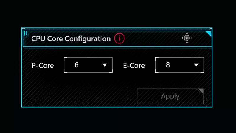
How to adjust your laptop's P-Cores and E-Cores for better performance and battery life
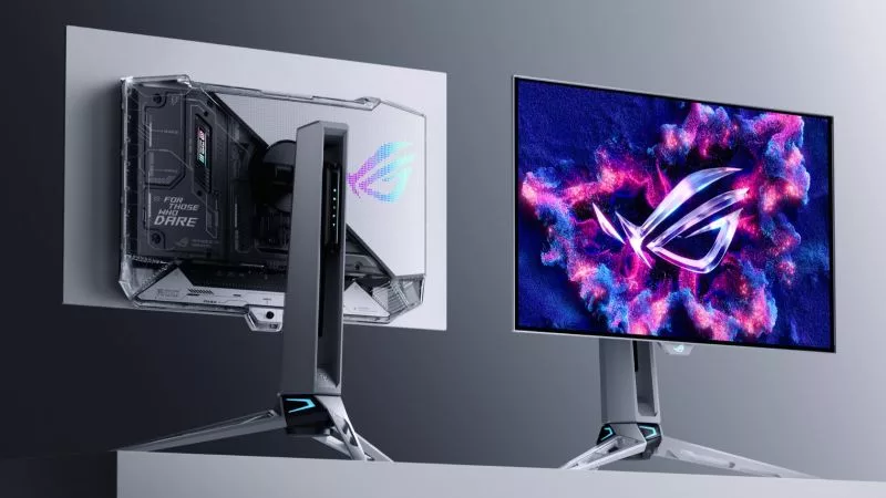
Prepare for Tandem OLED splendor with these new ROG gaming monitors
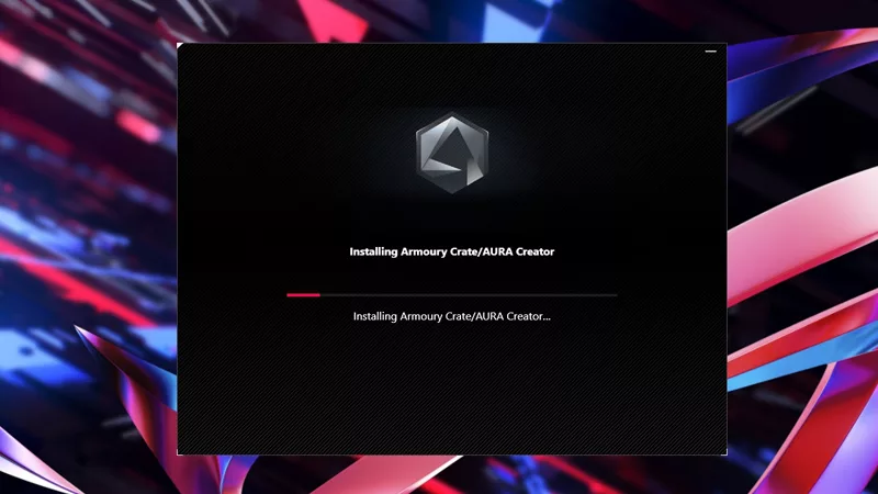
How to Cleanly Uninstall and Reinstall Armoury Crate
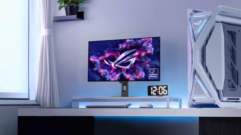
32-inch glossy WOLED panels debut in the ROG Strix OLED XG32UCWMG and XG32UCWG gaming monitors
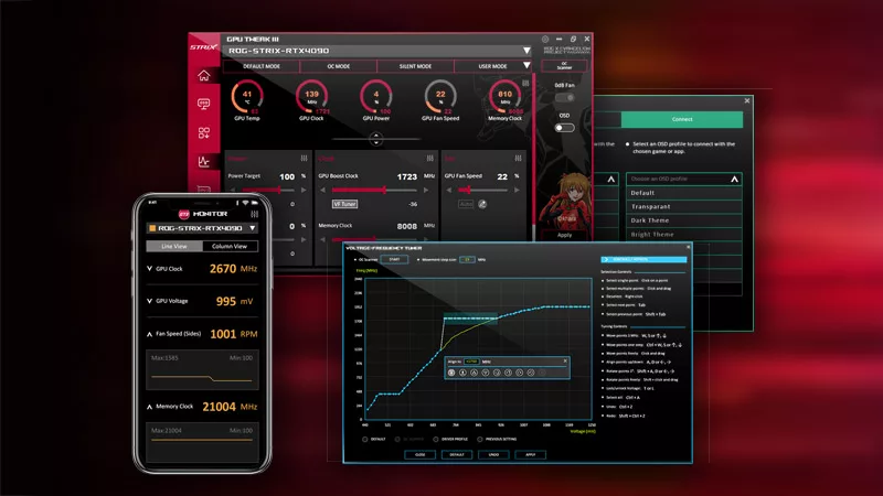
ASUS GPU Tweak III: The ultimate tool for advanced GPU tuning
LATEST ARTICLES
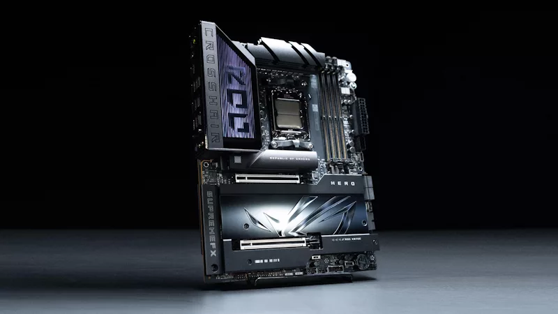
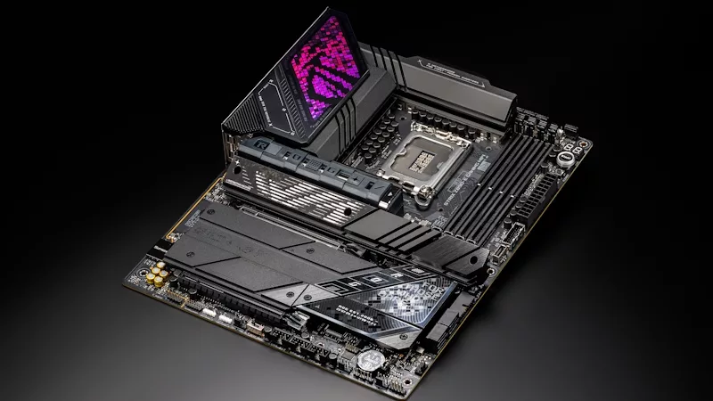
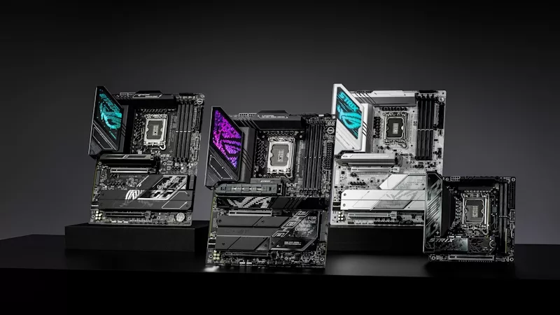
ROG Strix vs Extreme vs Apex vs Hero: What's the difference between ROG gaming motherboards?
When we launch a new generation of motherboards, we don’t just design one model and expect it to meet everyone’s needs. We give you a broad range of options from our ROG Maximus, Crosshair, and Strix lineups so that you can find the board for your next build.
Install up to seven M.2 SSDs on one motherboard with new ROG M.2 PowerBoost tech
Here's how ROG M.2 PowerBoost allows you to install more M.2 drives in one system while enjoying more stable performance.
ROG Z890 motherboard guide: meet the new contenders for your next gaming rig
New ROG Maximus and ROG Strix Z890 motherboards stand ready for your Intel Core Ultra (Series 2) CPU.
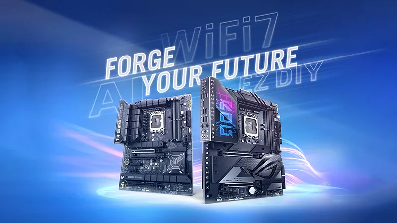
New Z790 motherboards from ROG pave the way for 14th Gen Intel Core CPUs
WiFi 7 support, more fast storage, front-panel device charging, intelligent controls — our latest Z790 motherboards have it all.
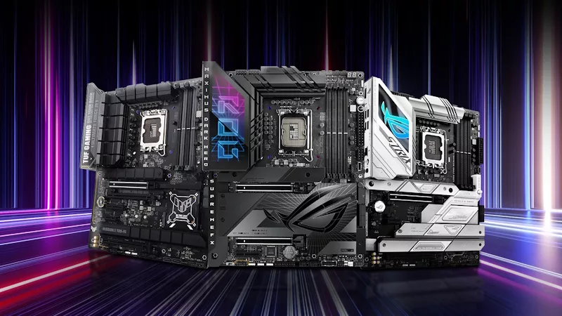
New Z790 motherboards from ROG pave the way for next-gen Intel Core CPUs
WiFi 7 support, more fast storage, front-panel device charging, intelligent controls — our latest Z790 motherboards have it all.
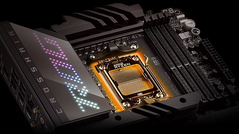
The best motherboards for a Ryzen 9 7950X3D CPU from ROG and TUF Gaming
AMD has released two new processors with 3D V-Cache technology: the Ryzen 9 7950X3D and the Ryzen 9 7900X3D. ROG and TUF Gaming X670 motherboards will provide a rock-solid foundation for these new top-tier chips.