Maximus V Formula LN2 OCing Preview From Shamino & Andre
While still 'in beta', ASUS pro overclockers, Shamino and Andre Yang show us the potentials of LN2 overclocking on the upcoming Maximus V Formula. These details are taken from the Kingpincooling thread, although you can discuss it in our own ROG forums here. Below, the explanations are in their own words:
Maximus V Formula OC Preview & Maximus V GENE Overclocking Demo
Firstly, to engage LN2 Mode, simply put a jumper at the location marked below:  LN2 Mode Enabled:
  The BIOS will show the 'Enabled' status and give you two Extreme OC Profiles that are suitable for users of Liquid Nitrogen. Profile 1 is more conservative and profile 2 is more aggressive.
  To make a simple ‘Slow-Mode’ switch, simply connect a wire from the spot marked below to a switch, with the other side of the switch being any local ground. Slow Mode is a common method used to make it easier to enter OS and validate results, etc
Points to watch when running LN2 Cooling for the best cold-bug free runs:
- Use a BCLK of 105MHz or higher
- Find the right CPU PLL Voltage that your CPU likes (can be higher or lower than default)
- Some CPUs may only initialize their high IMC Frequency at a warmer temperature though they may work fine after that
- A ‘23’ code when trying to boot means the CPU IMC is not able to run at that frequency at that temperature. A ‘30’ means the same as ‘23’ and a bit more.
- The highest DRAM Ratio known to be working = 2933 ratio
With the CPU and PSC chip DRAM under LN2, you can get the Maximus V Formula to churn out some crazy OC numbers, such as 2x2GB @ 3036MHz CL6-11-7-1T! [gallery include="" size="medium" link="file" template="file-gallery"] Power users love running low latencies, right? Do you miss the days of CL5, but still want today’s memory frequencies? How about CL5 @ 2400MHz!
 Maximus V Formula 2x2GB @ 2933MHz CL5-11-7-28 (What is CL5 good for? SuperPi 32M! Which you will see posted later. It requires lots of VDIMM and Elpida BBSE chips as cold as possible
A note on LN2’d DRAM
- PSC scales on cold but beyond that it's unnecessary and it might not even work too cold. Around -40ºC is enough to max out the DRAM and it may scale up to around ~1.95V.
- Elpida BBSE really scales on cold; the colder the better. Voltage scales up to ~2.30V
- Samsung are better just slightly chilled, with colder getting worse. Voltage scales up to ~2.20V
- Hynix scales on cold but beyond that it's unnecessary and it might not even work too cold. Around -40ºC is enough to max out the DRAM and it may scale up to around ~1.95V.

- PSC are almost always 2GB sticks, and typically have rated RAS to CAS Delay much higher than CAS, for eg 8-11-8, 9-11-9, etc
- Hynix presets are for 4GB sticks that are usually rated 2133MHz or more, and have slopping upwards and then downwards rated timing, such as 9-11-10, 10-12-11. They normally don’t scale much past 1.67v as well.
- Samsung presets are for 4GB sticks that are usually rated 2133MHz or more and have slopping upwards and then evening out rated timing, such as 10-12-12. They normally scale up to 1.80v and can do unusually low TRAS at high speeds, such as 21.
Even with fully loaded DRAM slots of 4x4GB, we've tuned the Maximus V Formula enough to run 4x4GB @ 3180MHz! [gallery include="" size="medium" link="file" template="file-gallery" columns="2"]
Maximus V Formula Memory OCing
Maximus V Formula 3200MHz POST screen with 4x4GB CL9. It goes straight to OS!  [video]http://www.youtube.com/watch?v=VMkctfBNWzs[/video]
Maximus V Formula 4x4GB @ 3220MHz CL9-12-12-31:
Maximus V Formula 4x4GB @ 3320MHz CL11:
Maximus V GENE Memory OCing
Maximus V GENE 2x4GB @ 3142MHz CL9, Command Rate 1T  Maximus V GENE @ 3000+MHz with G.Skill 2666MHz DDR3:
Maximus V GENE 4x4GB 2900MHz HyperPi stable with an air-cooled CPU!
Maximus V GENE 4x4GB @ 2876MHz CL9, Command Rate 1T  Maximus V GENE 4x8GB 2600MHz @ CL10 HyperPi stable with an air-cooled CPU!
Maximus V GENE 4x8GB @ 2933MHz, CL11 [gallery include="" size="medium" link="file" template="file-gallery" columns="2"] Maximus V GENE 4x8GB 2720MHz @ CL11 HyperPi stable with an air-cooled CPU! 
A few steps of advise to run SuperPi and PiFast on the Maximus V GENE:
- First we went into the BIOS and used: Load Extreme OC Profile 1
- Next we changed the CPU Ratio to 63x
- Then we chose the right profile for our PSC Memory and loaded the tight version of the Memory Profile.
- This sets our Latency Boundary at 1=> Tightest Third Timings since we are trying for best efficiency in SuperPi.
- We also changed VCore and Memory voltage accordingly.
- We saved and exited when the CPU Pot Temperature reached -100C.
- We entered the OS around -160C.
- We used Turbo V or ROG Connect to change the BCLK dynamically.
Here are the results: [gallery include="" size="medium" link="file" template="file-gallery"] 3D Mark 01:
The Latency Boundary:
We've picked out combinations of settings in the third set of memory timings that work well together to save you time. A setting of one will only work with very high performance DIMMs, although it will limit the overclocking frequency range. Hence a setting of two or higher will be required for most DIMMs when clocking past DDR3-2000. You can fine tune for performance in such a manner as well, such as after finding your stable memory clock speeds on auto, start by keying in ‘9’ and test for stability again. If its stable go down to ‘8’ and repeat. If its unstable go up to ‘10’ and test for stability again. Repeat in this manner. In this way you can find the fastest stable performance. 9 is typically the sweetspot for high ram speeds / performance compromise. A setting of around ‘3’ on Transmitter Slew may yield the best results and is a good starting point with most DIMM. Tweaking these settings will require some time, but can extend overclocking headroom for DRAM frequency. It’s best to adjust one step at a time and then run a memory intensive benchmark or stress test to monitor for changes in failure rates to find the optimal settings. After changing Transmitter Slew, one should go through the same steps tuning Receiver Slew. Both settings should be tuned before relying on an increase of voltage. For example Hynix ICs are typically like:  While Samsung ICs are typically like:
  You can disable DRAM Write Additional Swizzle to boot up at higher DRAM frequencies (especially if you see debug port code ‘55’), but it may affect stability and memory performance as well. Note: ‘55’ means the DRAM may be able to be tuned more, or the CPU IMC is capable but the DRAM is not. Whereas a ‘23’ means CPU IMC fails to initialize that that frequency. Use these as a process of elimination. You can tune for better performance by finding the best DRAM CLK Period for your configuration. A middle setting of ‘5’ may give best overall performance. BCLK Recovery means that the system will return BCLK to 100MHz when an OC failure is detected so disabling it will NOT return BCLK to 100MHz when OC failure is detected. This may save you some time when BCLK overclocking was not the cause of a POST failure.
Author
Popular Posts
How to adjust your laptop's P-Cores and E-Cores for better performance and battery life
How to Cleanly Uninstall and Reinstall Armoury Crate
Introducing the ROG Astral GeForce RTX 5090 and 5080: a new frontier of gaming graphics
How to configure your PC's RGB lighting with Aura Sync
How to upgrade the SSD and reinstall Windows on your ROG Ally or Ally X
LATEST ARTICLES
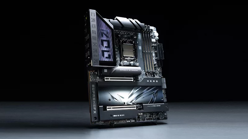
ROG Strix vs Extreme vs Apex vs Hero: What's the difference between ROG gaming motherboards?
When we launch a new generation of motherboards, we don’t just design one model and expect it to meet everyone’s needs. We give you a broad range of options from our ROG Maximus, Crosshair, and Strix lineups so that you can find the board for your next build.
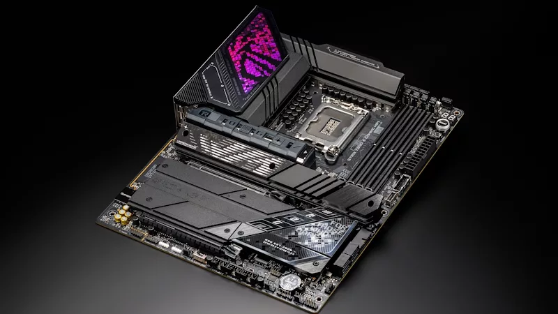
Install up to seven M.2 SSDs on one motherboard with new ROG M.2 PowerBoost tech
Here's how ROG M.2 PowerBoost allows you to install more M.2 drives in one system while enjoying more stable performance.
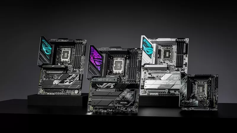
ROG Z890 motherboard guide: meet the new contenders for your next gaming rig
New ROG Maximus and ROG Strix Z890 motherboards stand ready for your Intel Core Ultra (Series 2) CPU.

New Z790 motherboards from ROG pave the way for 14th Gen Intel Core CPUs
WiFi 7 support, more fast storage, front-panel device charging, intelligent controls — our latest Z790 motherboards have it all.
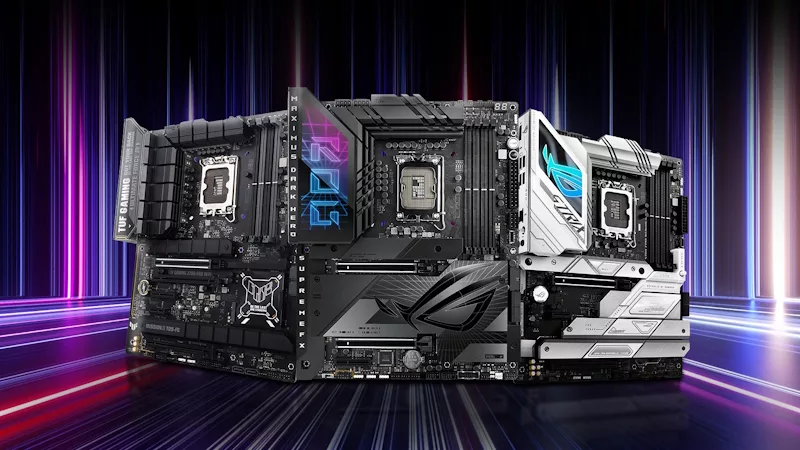
New Z790 motherboards from ROG pave the way for next-gen Intel Core CPUs
WiFi 7 support, more fast storage, front-panel device charging, intelligent controls — our latest Z790 motherboards have it all.
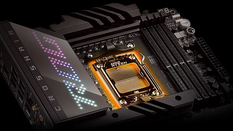
The best motherboards for a Ryzen 9 7950X3D CPU from ROG and TUF Gaming
AMD has released two new processors with 3D V-Cache technology: the Ryzen 9 7950X3D and the Ryzen 9 7900X3D. ROG and TUF Gaming X670 motherboards will provide a rock-solid foundation for these new top-tier chips.


