ASUS Z77 Motherboard UEFI BIOS Tuning Guide
This guide covers UEFI tuning for ASUS Z77 motherboards, including P8Z77 series, Sabertooth Z77 and Republic of Gamers Maximus V series. For the most part, the default auto settings for each parameter should suffice – we’ve selected optimum parameters for some of the more complex settings in order to allow users to achieve a successful overclock without too much fuss. If you are curious as to what some of settings do, or how/when they should be used, then you will find this guide of some use.
All of the overclocking related action takes place within the AI Tweaker Menu (UEFI Advanced Mode)

Ai Overclock Tuner:
Options are Auto, Manual and X.M.P.
Auto: This is the default setting, and needs to be changed to Manual if you wish to change BCLK (BCLK is the base reference frequency from which processor and other system bus frequencies are derived).
X.M.P:
Extreme memory profile, use this option if you have Sandy Bridge/Ivy Bridge qualified XMP memory.
X.M.P. profiles contain pre-sets for system buses and in some cases voltages. If the specified speed of the DIMMs is greater than the supported memory frequency of the platform, a platform specific X.M.P. profile option becomes mandatory because processor core and memory controller voltage requirements vary from architecture to architecture.
High-speed enthusiast memory kits manufactured before the inception of the Sandybridge/Ivy Bridge platforms may not contain the necessary/adequate voltage offset settings for the system to be completely stable. In such instances, manual adjustments of memory controller voltage and memory timings may be necessary.
It is also wise to purchase a single memory kit rated at the density and timings you wish to run rather than combining multiple kits to make up that density. The XMP profile and memory module SPD is configured by the memory vendor for a single kit only and does not take into account timing and voltage offsets that may be required for two or more kits to operate in tandem. One of the reasons that high frequency high density kits are more expensive than their lower density counterparts (even when the operating frequency and IC used is the same) is because the binning process at higher densities is more stringent – only a few ICs make the grade. Making a wise investment here will save frustration later on.
A final note on memory purchasing; Sandybridge processors are binned to run DDR3-1333 speeds at stock voltages (CAS 9). Higher operating frequencies are defined as overclocked, so voltage requirements and overall stability will vary from CPU to CPU. The same rule applies to Ivy Bridge processors, although the margin has been extended to DDR3-1600 at stock voltages for these CPUs. As such, unconditional stability at higher operating frequencies cannot be guaranteed and will vary between processor samples.
BCLK Frequency:
This function becomes available if X.M.P or Ai Overclock Tuner “Manual” are selected. The base BCLK frequency is 100MHz. The CPU core frequency is derived via multiplication with the Turbo Ratio setting (final frequency is displayed at the top-left of the Ai Tweaker menu). BCLK also adjusts memory operating frequency in association with the applied memory ratio (Memory Frequency and CPU bus speed: DRAM speed ratio mode settings below).
Bear in mind that the adjustment margin for this setting is not large - most processors have a range of 7 MHz +/- the base frequency, although there are some processor samples that can exceed this.
To make things easier, we’ve included an auto calculator which displays the target CPU and memory bus frequency for you in the top left area of the AI Tweaker menu:

ASUS MultiCore Enhancement:
When enabled sets ASUS defined Turbo core ramping policies. Disabled will apply Intel Turbo core ramping policies. For all overclocked configurations a setting of Enabled is recommended. Disabled can be used if you wish to run the processor within Intel guidelines when non-overclocked.
Turbo Ratio:
Options are “Auto”, “By All Cores” and “By Per Core”. A description of these settings is provided in the right-hand column of the UEFI BIOS and can be seen when the Turbo Ratio setting is selected.
By All Cores: This sets the CPU core frequency multiplier; multiplied by BCLK to give the target CPU frequency (under full load conditions if SpeedStep is active). “Auto” = stock CPU multiplier Ratio used. Manual numerical entry of the desired Turbo Ratio is accepted. *
Per Core: Allows setting the maximum Turbo multiplier of each physical processor core.*
*The available multiplier range is limited by both processor model and the ability of each CPU.
Internal PLL Overvoltage:
Increases internal phase locked loop rail voltage, allowing higher processor core frequency overclocking. A setting of Auto will enable this setting for you as you increase the CPU core multiplier over a certain threshold.
Most good processor samples will not need this setting enabled until overclocking past a core multiplier of 45X (4.5GHz CPU speed).
The stability of S3 sleep resume may be affected with this setting “Enabled”. If you find that your CPU won’t overclock past 4.5GHz without this setting Enabled, then the only choice may be to run at a lower speed if you find the system is unable to resume from S3 successfully.
CPU bus speed: DRAM speed ratio mode:
This setting is for Ivy Bridge processors only. This can be left at Auto to apply changes in accordance with the Memory Frequency setting.
Memory Frequency:
Selects the desired memory operating frequency (memory ratio). This setting is a derivative of BCLK and CPU bus speed:DRAM speed ratio mode. The target operating frequency is displayed within the drop-down list of this setting as well as the topleft corner of the Ai Tweaker menu.
Ivy Bridge CPUs have a wider range of memory ratio settings at their disposal than the previous generation Sandybridge processors. When used in addition with BCLK*, this allows more granular bus frequency control which should help us to tune a system to its full potential.
For daily use, we recommend opting for memory kits specified at a maximum of DDR3-1600.
Higher speed memory shows miniscule performance gains in most desktop software, so it is wiser to spend money elsewhere on the system. Further, the stability of the system at higher operating frequencies cannot be guaranteed, often interfering with resume from sleep states and also when the system is stressed by software. Hence our advice to opt for memory kits that are within processor specifications if you do not wish to spend time tuning the system for stability.
At the other end of the spectrum, benchmarking fanatics will find that 2GB PSC based kits offer the best overall performance in memory sensitive benchmarks. Target operating frequencies between DDR3-2400 to DDR3-2600 seem to be the optimal point for best scores and times in sensitive benchmarks utilizing CAS 6 or 7 timing sets, in tandem with sub-zero cooling of both the processor and memory modules. Higher speeds are possible at the expense of secondary and third memory timing parameters, often at the expense of efficiency. If PSC based kits are not available, then Samsung based kits offer a modern alternative albeit requiring looser operating latency at equivalent frequencies.
*Within functional limits of the BCLK setting.
iGPU Max. Frequency:
Sets the operating frequency of the on-die GPU.
EPU Power Saving Mode:
Auto adjusts system operating frequency and voltage regulation settings in order to save power. This setting should only be enabled at stock processor operating frequency. For all overclocking use, a setting of Disabled is recommended.
OC Tuner:
When enabled will run a series of stress tests during the POST-Boot process in order to auto-overclock the system. The final overclock will vary according to system temperatures and the memory kit used. Enable only if you do not wish to manually overclock the system.
DRAM Timing Control:
Takes us to the DRAM Timing sub-section:
Most of these settings can safely be left at Auto unless you wish to tune the system for optimal scoring in benchmarks. The primary timings will be set in accordance with the memory module SPD at a given frequency or fall back on ASUS defaults as memory bus frequency is increased.

DRAM CAS Latency:
Column Address Strobe, defines the time it takes for data to be ready for burst after a read command is issued. As CAS factors in almost every read transaction, it is considered to be the most important timing in relation to memory read performance. To calculate the actual time period denoted by the number of clock cycles set for CAS we can use the following formula:
tCAS in Nano seconds=(CAS*2000)/Memory Frequency
This same formula can be applied to all memory timings that are set in DRAM clock cycles.
DRAM RAS TO CAS Latency:
Also known as tRCD. Defines the time it takes to complete a row access after an activate command is issued to a rank of memory. This timing is of secondary importance behind CAS as memory is divided into rows and columns (each row contains 1024 column addresses). Once a row has been accessed, multiple CAS requests can be sent to the row the read or write data. While a row is “open” it is referred to as an open page. Up to eight pages can be open at any one time on a rank (a rank is one side of a memory module) of memory.
DRAM RAS# PRE Time:
Also known as tRP. Defines the number of DRAM clock cycles it takes to Precharge a row after a page close command is issued in preparation for the next row access to the same physical bank. As multiple pages can be open on a rank before a page close command is issued the impact of tRP towards memory performance is not as prevalent as CAS or tRCD - although the impact does increase if multiple page open and close requests are sent to the same memory IC and to a lesser extent rank (there are 8 physical ICs per rank and only one page can be open per IC at a time, making up the total of 8 open pages per rank simultaneously).
DRAM RAS Active Time:
Also known as tRAS. This setting defines the number of DRAM cycles that elapse before a Precharge command can be issued. The minimum clock cycles tRAS should be set to is the sum of CAS+tRCD+tRTP.
DRAM Command Mode:
Also known as Command Rate. Specifies the number of DRAM clock cycles that elapse between issuing commands to the DIMMs after a chip select. The impact of Command Rate on performance can vary. For example, if most of the data requested by the CPU is in the same row, the impact of Command Rate becomes negligible. If however the banks in a rank have no open pages, and multiple banks need to be opened on that rank or across ranks, the impact of Command Rate increases.
Most DRAM module densities will operate fine with a 1N Command Rate. Memory modules containing older DRAM IC types may however need a 2N Command Rate.
Secondary Memory Timings
DRAM RAS to RAS Delay:
Also known as tRRD (activate to activate delay). Specifies the number of DRAM clock cycles between consecutive Activate (ACT) commands to different banks of memory on the same physical rank. The minimum spacing allowed at the chipset level is 4 DRAM clocks.
DRAM Ref Cycle Time:
Also known as tRFC. Specifies the number of DRAM clocks that must elapse before a command can be issued to the DIMMs after a DRAM cell refresh.
DRAM Write Recovery Time:
Defines the number of clock cycles that must elapse between a memory write operation and a Precharge command. Most DRAM configurations will operate with a setting of 9 clocks up to DDR3-2500. Change to 12~16 clocks if experiencing instability.
DRAM Read to Precharge Time:
Also known as tRTP. Specifies the spacing between the issuing of a read command and tRP (Precharge) when a read is followed by a page close request. The minimum possible spacing is limited by DDR3 burst length which is 4 DRAM clocks. Most 2GB memory modules will operate fine with a setting of 4~6 clocks up to speeds of DDR3-2000 (depending upon the number of DIMMs used in tandem). High performance 4GB DIMMs (DDR3-2000+) can handle a setting of 4 clocks provided you are running 8GB of memory in total and that the processor memory controller is capable. If running more than 8GB expect to relax tRTP as memory frequency is increased.
DRAM Four Activate Window:
Also known as tFAW. This timing specifies the number of DRAM clocks that must elapse before more than four Activate commands can be sent to the same rank. The minimum spacing is tRRD*4, and since we know that the minimum value of tRRD is 4 clocks, we know that the minimum value for tFAW at the chipset level is 16 DRAM clocks.
As the effects of tFAW spacing are only realised after four activates to the same DIMM, the overall performance impact of tFAW is not large, however, benchmarks like Super Pi 32m can benefit by setting tFAW to the minimum possible value. As with tRRD, setting tFAW below its lowest possible value will result in the memory controller reverting to the lowest possible value (16 DRAM clocks or tRRD * 4).
DRAM Write to Read Delay:
Also known as tWTR. Sets the number of DRAM clocks to wait before issuing a read command after a write command. The minimum spacing is 4 clocks.
As with tRTP this value may need to be increased according to memory density and memory frequency.
DRAM CKE Minimum Pulse width:
This setting can be left on Auto for all overclocking.
CKE defines the minimum number of clocks that must elapse before the system can transition from normal operating to low power state and vice versa.
DRAM RTL & IOL:
Unlike other timings, DRAM RTL and IOL are measured in memory controller clock cycles rather than DRAM bus cycles. These settings can safely be left on Auto for all normal use. The RTL and IOL define the number of memory controller cycles that elapse before data is returned to the memory controller after a read CAS command is issued. The IOL setting works in conjunction with RTL to fine tune DRAM buffer output latency. Both settings are auto-sensed by the memory controller during the POST process (memory training). Manual adjustment should not be necessary unless the system is being used in order to obtain maximum DRAM frequency screenshots (limited stability).
Tertiary Memory Timings

Most of these timings can be left on AUTO unless tweaking for SuperPi 32M. The best way to tune these settings if benchmarking is to set them to their maximum value and then decrease one step at time while monitoring stability at every change. We have color-coded text within this section to highlight more important timings over lesser ones.
Red = more important
Black = less important
tRRDR (DD):
Sets the read to read delay where the subsequent read requires the access of a different rank on a different DIMM. 3 clocks will work with most configurations at high memory frequencies.
tRWDD (DD):
Sets the delay period between a read command that is followed by a write command; where the write command requires the access of data from a different rank or DIMM. A setting of 3 clocks suits most DIMM configurations all the way to DDR3-2133. Relax to 5~7 clocks only if you are experiencing stability issues when running in excess of 8GB of memory over DDR3-2300.
tRWSR:
Sets the delay between a read command followed by a write command to the same rank.
tRR (DD):
Sets the read to read delay where the subsequent read requires the access of a different DIMM. 3 clocks will work with most configurations.
tRR (DR):
Sets the delay between read commands when the subsequent read requires the access of a different rank on the same DIMM.
tRRSR:
Sets the delay between read commands to the same rank. A setting of 4 clocks is preferred for benchmarking, increase only if experiencing instability.
tWW(DD):
Sets the write to write delay where the subsequent write requires the access of a different DIMM. 3 clocks will work with most configurations, increase if using 4GB or 8GB DIMMs with all slots populated.
tWW(DR):
Sets the write to write delay where the subsequent write command requires the access of a different rank on the same DIMM, increase if using 4GB or 8GB DIMMs with all slots populated.
tWWSR:
Sets the delay between write commands to the same rank. A setting of 4 clocks is preferred from a performance perspective; however this may need increasing in tandem with memory frequency to maintain stability.
Misc Memory Settings

MRC Fast Boot:
Bypasses longer memory training routines during system re-BOOT. Can help speed up BOOT times. If using higher memory frequency divider ratios (DDR3-2133 and over), then disabling this setting while trying to achieve stability can be beneficial. Once the desired system stability has obtained, Enable this setting to prevent the auto sensed parameters from drifting on subsequent system re-BOOTs.
DRAM CLK Period:
Defines memory controller latencies in conjunction with the applied memory frequency. A setting of 5 gives best overall performance though may impact stability.
Transmitter Slew & Receiver Slew:
A setting of around ‘3’ on Transmitter Slew may yield the best results or a good starting point with most DIMM. Tweaking these settings will require some time, but can extend overclocking headroom for DRAM frequency. It’s best to adjust one step at a time and then run a memory intensive benchmark or stress test to monitor for changes in failure rates to find the optimal settings.
After changing Transmitter slew, one should go through the same steps tuning Receiver Slew. Both settings should be tuned before relying on an increase of voltage.
MCH Duty Sense CHA & CHB:
These settings can be left on Auto most of the time. If experimenting, start at middle value of 15, check for impact on stability then move up by +2 and re-check. Tuning will be system and DIMM specific and depend on operating frequency.
CHA & CHB DIMM Control:
Allows a user to disable a channel without physically removing the DIMM. Leave on Auto unless experimenting or testing individual channels for stability.
DRAM Read and Write Additional Swizzle:
Leave these settings on Auto unless experiencing instability at high DRAM frequency. Toggling from enabled to disabled or vice-versa may help pass a benchmark where the DIMMs were otherwise unstable.
CPU Power Management:

Takes us to a sub-menu that allows configuration of non-Turbo ratio CPU multipliers as well as set power thresholds for Turbo multipliers. Information is provided within UEFI with regards to the usage of each option.
DIGI+ Power Control:
Each of the settings within the DIGI+ VRM section has an explanation listed in the right hand column of UEFI. All settings have been configured to scale on Auto in accordance with overclocking. We’ll highlight some settings below for clarification purposes.
Load-Line Calibration:
AKA LLC, sets the margin between applied and load voltage. For 24/7 use a setting of 50% is considered optimal, providing the best balance between set and load voltage in a manner that compliments the VRM for all loading conditions. Some users prefer using higher values, although this will impact overshoot to a small degree.
VRM Spread Spectrum:
ssigns enhanced modulation of the VRM output in order the peak magnitude of radiated noise into nearby circuitry. This setting should only be used at stock operating frequency, as the modulation routines can impact transient response.
All “Current Capability”settings:

A setting of 100% on all of these settings should be ample to overclock processors using conventional cooling methods. If pushing processors using LN2 or other sub-zero forms of cooling then increase the current threshold to each voltage rail respectively. A setting of 140% should ensure OCP does not trip during benchmarks.
CPU Voltage:
There are two ways to control CPU core voltage; Offset Mode and Manual Mode. Manual mode assigns a static level of voltage for the processor. Offset Mode allows the processor to request voltage according to loading conditions and operating frequency. Offset mode is preferred for 24/7 systems as it allows the processor to lower its voltage during idle conditions, thus saving a small amount of power and reducing unnecessary heat.
The caveat of Offset Mode is that the full load voltage the processor will request under load is impossible to predict without loading the processor fully. The base level of voltage used will increase in accordance with the CPU multiplier ratio. It is therefore best to start with a low multiplier ratio and work upwards in 1X steps while checking for stability at each increase. Enter the OS, load the CPU and check CPU-Z to check the voltage the CPU requests from the buck controller. If the level of voltage requested is very high, then you can reduce the full load voltage by applying a negative offset in UEFI. For example, if our full load voltage at 45X CPU multiplier ratios happened to be 1.40V, we could reduce that to 1.35V by applying a 0.05V negative offset in UEFI.
Most of the information pertaining to overclocking Sandy Bridge CPUs has already been well documented on the internet. For those of you purchasing retail Ivy Bridge CPUs, we expect most samples to achieve 4.3-4.5GHz with air and water cooling. Higher overclocks are possible although full-loading of the CPUs will result in very high temperatures even though the current consumed by these processors is not excessive. We suspect this is a facet of the 22nm process.
iGPU Voltage:
Sets the rail voltage of the integrated GPU. Same function as CPU Vcore with regards to Manual and Offset Mode.
DRAM Voltage:
Sets voltage for the memory modules. 1.50V DIMMs qualified on Sandybridge and Ivy Bridge processors are recommended for use on this platform.
VCCSA Voltage:
Sets the voltage for the System Agent. It can be left on Auto for most overclocking.
VCCIO:
May need adjustment on Sandybridge processors if using 16GB of memory or memory modules that contain ICs that represent a tough load to the memory controller. 1.05V is base, if adjusting increase in 0.025V steps and check stability at each increment.

CPU PLL Voltage:
For most overclocking, the minimum voltage requirements will be centered around 1.80V. If using higher processor multiplier ratios or DRAM frequencies over DDR3 2200, then a small over-voltage here can aid stability. Don note that the processor will become increasingly sensitive to PLL voltage changes at sub-zero temperatures and when nearing the maximum frequency the CPU is capable of.
PCH Voltage:
It can be left at default values for all overclocking. We have not observed any relationship between this voltage rail and any other in our testing to date.
DRAM DATA and CTRL References for all channels:
Allow adjustment of the DRAM read/write reference voltages for the DATA and CTRL signal lines. A setting of Auto defaults to 50% of VDIMM which should be adequate for almost all overclocking. Adjustment can sometimes be required when benchmarking memory at very high operating frequencies. In such instances a small reduction or increase (one step) above or below 50% can help aid stability in memory intensive benchmarks. Also if processors are sub-zero cooled, there may come a point where the memory controller becomes unstable regardless of operating frequency. This is where fiddling with these voltages can sometimes help pass benchmarks that would be otherwise unstable.
CPU Spread Spectrum:
Modulates processor core frequency in order to reduce the peak magnitude of radiated noise emissions. We recommend setting this to disabled if overclocking the as the modulation can interfere with system stability.
BCLK Recovery:
When enabled, this setting will return BCLK to a setting of 100 MHz (default) if the system fails to POST. Disabling it will NOT return BCLK to 100MHz when OC Failure is detected.
Author
Popular Posts
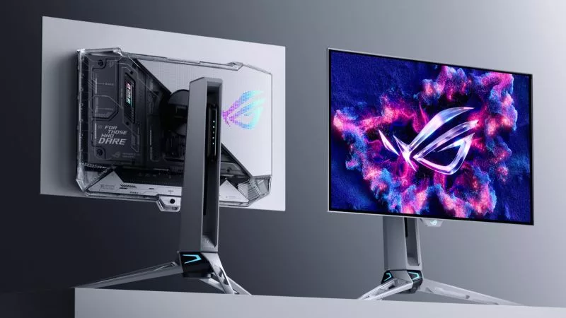
Prepare for Tandem OLED splendor with these new ROG gaming monitors

The ROG XREAL R1 gaming glasses let you game anywhere on a 171-inch 240Hz virtual screen
How to Cleanly Uninstall and Reinstall Armoury Crate
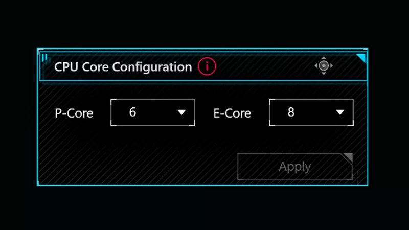
How to adjust your laptop's P-Cores and E-Cores for better performance and battery life
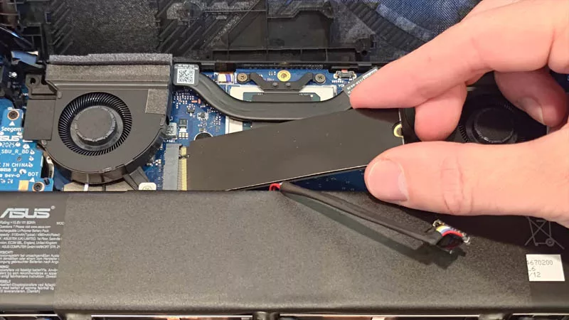
How to upgrade the SSD and reinstall Windows on your ROG Ally, ROG Xbox Ally, or ROG Xbox Ally X
LATEST ARTICLES
Here come the ROG and ASUS GeForce RTX 2070 graphics cards
Our NVIDIA GeForce RTX 2070 cards pair real-time ray tracing and artificial intelligence with cutting edge gaming and VR performance.

Gallery: BlizzCon Celebrates 10th Anniversary with ASUS and ROG
Since BlizzCon is also celebrating its 10-year anniversary, why not celebrate together?

ASUS ROG to Join LAN ETS in Canada
The biggest LAN party in Canada is here! HWBOT World Tour will also be there, don't miss out!

ASUS Straight Edge Podcast: Episode 3 - CPU Q&A with Intel
Intel PR manager Dan Snyder, and strategic marketing lead for enthusiasts, Aaron Mcgavock have 40 years of experience at Intel between them, Dan and Aaron have lots of insights related to tech and media to share. We present our questions and yours, to dig deep and get the nitty gritty details. Don't miss this!
AnandTech Looks Back at 10 Years of ROG
AnandTech has had a direct line of communication with ROG since the beginning. Let's take a look back at how ROG and AnandTech have evolved and what lies ahead. Don't miss the Q&A as AnandTech readers had the opportunity to have their say!