Memory Overclocking Guide For Rampage IV Black Edition (Beginner To Advanced)
Originally posted in our forums by tech guru, Raja, this guide is aimed at those looking to maximize their overclocking and tweaking performance on the new Rampage IV Black Edition. It suits anyone from beginner to advanced, so everyone should get something out of it!
Memory Overclocking Guide For Rampage IV Black Edition
This guide provides basic information on how to overclock the Rampage IV Black Edition (R4BE) motherboard and also information on overclocking in general. Whether you’re using an R4BE motherboard or not, there are some valuable learning tips in this guide that help understand the process of stable overclocking on any platform – read on! For those of you using Ivy-E there’s already a basic processor overclocking guide here. We’d recommend reading through that overclocking guide in its entirety before continuing here. In this memory guide, we provide further information on settings and basic methodology to help obtain a stable system overclock. The R4BE is a high performance X79 chipset based motherboard, tuned to extract maximum performance from Intel’s Ivy-E processors. Our engineers have tweaked trace layout and components to improve quad channel DRAM overclocking potential over first generation X79 motherboards. DRAM signal line matching is improved between channels and slots, impedance has been changed to suit Ivy-E processors, while DRAM power components have been upgraded over the Rampage 4 Extreme to provide even better regulation. As a result, there are certain situations in which the R4BE can run tighter DRAM timings than the R4E or other X79 boards at equivalent voltages. Success, as always, depends largely on having a good combination of parts while the rest comes down to using a systematic approach of getting from stock to an intelligently tuned overclock.
Methodology Basics
This guide assumes you are running UEFI BIOS version 0507 or later. By default, UEFI parameters that relate to overclocking have automated scaling routines embedded in the background that will change/increase voltages to facilitate overclocking. In other words, we can simply change the processor multiplier ratio (within realistic limits), apply XMP for DRAM and let the board do the rest. However, there are processors and DRAM kits that may need special tuning for full stability. Either the CPU needs more voltage than average for a given frequency, or perhaps the DRAM modules being used aren’t stable at the timings or memory controller voltages the board applies on Auto. It’s the methodology for getting through these situations we’ll focus on today. One common mistake we deal with on forums relates to users trying to push processors too far, too soon. New users come to forums, have a look around and focus on copying the best overclocking results they can find; expecting their own processors to reach the same frequency as matter of course. Unfortunately, the system ends up being unstable, with the user frustrated and unsure of why there is an issue, or what needs to be adjusted. We can therefore conclude that a non-systematic approach to overclocking, leaves us with no clue about what to adjust when faced with instability: is the system unstable because CPU core voltage is too low? Is it related to DRAM? Could it be that the processor memory controller (IMC) can’t handle high DRAM speeds? It could be any and all of these at the same time, or it could simply come down to having a worse CPU sample than “KingD”, who was either really lucky, or he purchased multiple CPUs to find a good one. That’s why using a systematic and gradual approach is advised by us – use the results of others as a reference but don’t be fooled into thinking your parts can do the same simply by copying settings. So what’s systematic and gradual in the context of overclocking? Well, it includes methods to focus on certain parts of the system to evaluate overclocking potential before shooting for the moon. We can use different types of stress tests to focus on the CPU cores, and we can also use programs that focus more on memory to get a feel of what is possible on our combination of parts. Once we’ve got a feel for how things react, we can add more comprehensive forms of stress testing to evaluate the system as a whole. We should stress that it is imperative to perform a basic evaluation of stability before attempting any type of overclocking on the system. Leave everything at default parameters and check the system is stable and working as it should be. A tool like ROG Realbench is perfect for this task, allowing us to check stability in a manner akin to real-world applications and system loads. We should also install a third party temperature application at this stage to check CPU and system temperatures are within comfortable bounds at idle and when the system is under load. If anything is running too hot, or is unstable, it’s pointless trying to overclock the system without attending to the issue first. If the system is stable at stock speeds and has suitable overhead in terms of temperature, we can move to overclocking the system. The process is best started by isolating one side of the processor before overclocking the system as a whole unit. As an example, we can use various memory stress tests to evaluate how good our memory modules are and how good the memory controller in our CPU sample is. This is especially important for those of us that purchase high-speed memory kits. It’s possible that the processor is perfectly stable with little manual adjustment of voltages at high memory speeds, but it’s also possible the memory controller in our sample needs voltage or memory timing adjustments to be stable. At worst, the memory controller could be completely unstable at the desired operating frequency regardless of adjustments, in which case we have to accept a lower operating point. The latter can be debilitating to realize if one has purchased a high performance and expensive memory kit. Such things do happen. Once we’ve determined the memory can run at a given frequency, we can set a lower memory operating frequency for sake of isolating the CPU to find its overclocking potential. This eliminates guesswork as the memory will almost certainly be unconditionally stable at a lower operating speed, giving us fewer variables to fight against as we evaluate overclocking potential of the CPU cores. At this stage, we use a stress test routine that focuses primarily on the CPU. We can increase the CPU multiplier ratio by 1 and then see what kind of voltage the CPU needs to be stable. Once the required voltage for stability at the new frequency is found, we can again increase the multiplier ratio and repeat the stability testing and voltage tuning process. Keeping notes is valuable at this stage and will show a near linear pattern of voltage versus frequency increase. Eventually, we arrive at a point where we’ve either run out of cooling potential (temps are too high), or we need to make a huge voltage increase to get the processor stable. This is where I personally back off, and select the lower operating point. Why? Because the current drawn by the processor is proportional to voltage and operating frequency. Choosing the lower point is kinder to the processor from a longevity standpoint and there’s a better chance the system will remain stable over the long-term.
A few Overclocking Technicalities Analogized
Why does a system become unstable when it is overclocked? There are numerous reasons, actually. More than one could cover in a single article. Many require electrical engineering backgrounds to both write and to understand. Electrical engineers we are not… Well, most of us (including me) are not anyway, so we’re going to try and keep things simple. Fundamentally, the role of a processor is to calculate, write and read data. At the core level, this data is represented and moved around the system as 1’s and 0’s (binary patterns). Let’s look at a crude visual representation of how data is represented at the electrical level:  The “wavy” line is the signal alternating between a high and low voltage to represent 1 and 0. In this brief example the data pattern being transmitted from the memory bus to the processor is 101010.
- VOH (voltage output high) is the high voltage output level of the transmitter that represents a logic 1, while VOL is the low output voltage (voltage output low) representing a logic 0.
- VREF is the reference voltage. The reference is typically set at the midpoint between VOL and VOH.
- VDDQ (not shown, and known as DRAM Voltage on motherboards) is the voltage supply for VOH, VOL and the voltage from which VREF is derived.
Most signal stages have three states: VOH, VOL and “off” - known as a tri-state transceiver/s. Typically, “off” state will be a certain level lower than VOL but above ground potential. The off state is required to prevent inadvertent data transmission. This standing voltage (bias) in “off” state is attached to a compensation network to hold the voltage below VOL when the signal line is not transmitting. Compensation is usually in the form of a resistor to ground, but can be something more elaborate if required. The reason a certain level of bias is present and the line it is not at ground potential in “off” position is due to a number of factors which fall outside the scope of this article. For this example, let us assume VOH is around 80% of VDDQ, VOL is 20% of VDDQ, while VREF is 50% of VDDQ. The signal swings between VOL and VOH to represent data as a 1 or 0 while a strobe compares the signal against VREF. If the voltage is higher than VREF determines it to be a logic 1, or if the signal voltage is below VREF it is interpreted as a logic 0. Needless to say, the process of transferring the data and interpreting it accurately requires that the transmitter and the receiver device be in close timing sync. If there is a lack of synchronization between the transmitted signal and the strobe, the data could be read erroneously. In the ideal world, the signal waveform would be perfectly symmetrical as it transitions between high and low states. Never crossing above VOH or below VOL. The keen eyed among you will notice in the diagram above that the signal varies slightly from one transition to the next. That’s mostly because I’m crap at drawing, but in this case, fortunately, the rendition fits! The waveforms are non-symmetrical and have different levels of excursion past VOH or VOL (overshoot and undershoot). There are various reasons why these issues occur; power supply fluctuation, jitter, impedance issues and noise just to name a few. We won’t go into all of the factors leading to these problems as many fall outside the scope of this article. However, we can break down what happens as a result of them by using a real-world analogy in a context we can relate to.
Analogy Number One: Data Sampling and Conveyer Belts…
One could use the analogy of a conveyer belt and a strobe light to visualise the process of sampling data. Boxes are placed on a conveyer belt and a strobe light is used to highlight a barcode on the box to take a recording of the number printed on it. As the box moves past the flashing strobe light, the light turns on to look at the barcode. If the timing between the strobe and the box is not in sync, the strobe will flash to take a sample when the box is not in the ideal position – leading to a misread. Suppose we want to speed up production (overclocked production); we increase the speed of the belt and the speed of the machine that places the boxes on the belt to do so. However, we soon hit a few snags. At high speed, the machine that places boxes onto the belt may not place them perfectly square, or there may be timing issues where the gap between the boxes varies. This eats into the available sampling margin for the strobe and there comes a point where the barcode on a box cannot be read accurately. In effect, this is very similar what happens as we overclock a system – waveform integrity starts to suffer and we lose margin to sample or transfer data. We can counter some of this by increasing or tuning voltages, altering memory timings and by improving system cooling (for lower temperatures of critical areas). The impact of voltage changes to various portions of a processor can have different effects. Take CPU Vcore for example, we know that it has to be increased as we raise the frequency of the processor cores to any appreciable degree. We are asking the processor to “switch” faster and voltage provides the potential for that to happen. The electrical process behind this is a lot more complex than our statement, but in the real world the fact holds that CPU core overclocking is primarily reliant on increased voltage and to various degrees (excuse pun) on low processor temperature. We can also apply the same rule to the processor’s memory controller or memory modules – although not quite to the same extent. Why? Well, the role of what voltage does to portions of the memory sub-systems can be more delicate; there are instances in which more voltage is not the answer…
Overshoot, Ringback and Undershoot
Let’s roll back to our earlier “data” image:  If one were to look at the waveform at increased resolution on a scope, it is likely that the portions of the waveform showing overshoot would look something like this:

- Enlarged view showing VOH (logic 1) overshoot and ringback
In signalling language, the term overshoot refers to a signal excursion beyond a defined level. In our images the defined level for a logic 1 (high level) is VOH. The images above show a signal that has breached VOH and then recovers oscillating slightly (ringback) before returning to a logic 0. Similarly, undershoot refers to a signal that falls below an ideal level. Overshoot and undershoot occur to a greater degree when the device responsible for generating the signals (transistor stages) is run outside comfortable operating limits. Transistors have an ideal voltage region in which they operate in a predictable manner; when we increase voltage and ask them to switch faster, we push them outside that region which can lead to unpredictable behaviour. This is the reason why processors have stipulated supported operating speeds. The processor vendor spends a great deal of time evaluating the guaranteed and safe operating limits of their CPUs at frequencies, voltages and power consumption levels that ensure stability and acceptable lifespan. The horizontal axis in these illustrations represents time. If the signal overshoots or undershoots the expected level (VOH or VOL), the time it takes to transition between high and low states is affected and this eats into the available timing budget because the sampling signal (strobe) may not be experiencing exactly the same problem. If the time difference between the DQ signal and strobe is too wide, a signal could be seen as a logic 1 instead of a 0 or we may simply run out of timing budget for any kind of data transfer. The faster the system is running in frequency, the more chance there is of such issues. As a result, we have a smaller and smaller timing budget to play with as we overclock a system, until we eventually run out of overhead and things become unstable.
Analogy Number Two: One Man, One Ball and a Wall….
There’s no simplistic way to explain the intricacies of signalling, as the scope of this subject is HUGE. In fact, there’s no single real-world analogy that can be used either, as there are too many contributors and detractors to the integrity of a signal. So, we’ll aim for a small degree of the picture with limited accuracy. Probably enough to raise more questions than it answers, so please keep an open mind as what follows is by no means absolute. You certainly don’t want to walk into a university lecture for EE students, waving your finger around claiming to understand the depths of signalling thanks to our wonderful analogies Ball game: One person throws a ball over a defined distance at a target painted on a wall which then bounces off the wall and must be caught in order to throw it again. As we’re relating this to overclocking, there are some caveats to the game:
- In order to meet our timing budget, 10 throws at the target must be completed in 10 seconds. We can relate these 10 throws to frequency – obviously bearing in mind that computer systems operate at many thousand “throws” per second.
- Voltage supplies the potential or strength to throw the ball. Higher voltage levels equate to a faster and more powerful throw.
- If throwing power (voltage) is excessive it affects throw accuracy and the ability to catch the ball when it rebounds.
- If throwing power (voltage) is not sufficient it may not be possible to make enough throws in the designated time. It may also not be sufficient to reach the target accurately.
- Failure to hit the target or close to the target results in the ball returning to the thrower in a non-ideal path, negatively affecting time between each cycle.
If we are fortunate enough to have an imagination that can visualise this game, we’ll understand that there are quite a few constraints and a growing potential for issues as we increase the number of throws that need to be made within a given timeframe. Overclocking any bus on a system is riddled with issues similar to this and many more. In this instance, we’ve just begun to touch on the relationship between signal integrity and voltage. In the real world, if we apply too much voltage to signal stages, we risk signal integrity and possible damage to the transistors that swing the signal. However, we also need to supply enough voltage to ensure the signal slew rate (acceleration of a signal is defined as slew rate) is sufficient to meet timing requirements. In other words, too much voltage can be harmful and induce instability. Similarly a voltage level too low can also incite instability, although there’s less chance of processor damage if we stick closer to “stock” voltage levels. The settling limit time budget is the maximum deviation the signal can suffer when recovering from overshoot. If the signal breaches the settling time limit, we are effectively outside reliable sync with the strobe and the system becomes unstable.
The Part that Parts Play
CPU memory controller quality and motherboard design also affect settling time budget. If the memory controller is a good sample, it will not suffer as much overshoot or require as much voltage as a weaker sample to operate reliably at a given frequency. Trace layout of the motherboard can help in that area too – if traces are well length matched with a suitable impedance for the memory controller and memory module output stages to drive signals into, we get more overhead to play with before we run out of overclocking headroom. Hence we can overclock portions of the system at lower operating voltages than less-optimized solutions. The synchronization process of signal lines takes place during POST. The memory controller sends data patterns to the memory banks and then adds a delay to, or advances the signal to ensure associated lines are closely matched. Binary patterns used for this process can be just as strenuous as running a short stress test on the system. The role of this test is to generate data patterns that cause current swings on the memory system – which stresses power circuitry, transceiver stages and causes near worst case noise on signal lines. Signal timing is then adjusted, together with voltage references to centralize waveforms against data sampling stages to ensure excellent stability in most scenarios – at least until we start pushing a system to its limit. This also explains why motherboards don’t POST or fail to map DIMMs when memory stability is an issue. If memory frequency is too high, voltages are not adequate, or there is simply no overhead left in the parts being used, the POST process will find an error and may either halt, or fail to map a memory rank. Such things are not easy to fix for users that are not well versed in overclocking. As a result, our “highly responsible” advice is to purchase parts that keep the processor within a comfortable operating range. As stated earlier, transistor behavior becomes more erratic as we overclock the system, and the system as a whole more sensitive to interference or other signal affecting nasties. Even if we’re transmitting the same binary pattern over and over, the signal artifacts can be random in nature. A load transient on the power supply, random radio frequency or electromagnetic interference can all influence signal integrity as we run a system closer to its clock limits. There are more complex issues that rear their head for stability, too. Temperature affects the impedance of motherboard traces and the ability of transistors on the processor or memory modules to swing voltage. Most conductive materials have what is called a temperature co-efficient, which means their resistance varies with temperature. This drift in trace impedance or in the permeability of silicon can lead to changes in signal quality. To counter these problems, modern processor architectures employ different types of POST training routines at cold AC power cycle and warm reset. As always, these routines are designed to run reliably at stock operating parameters. When a system is overclocked near its limits, the drift in parts and the training mechanisms themselves can be enough to prevent POST from AC cycle or cause issues with system resets – even if the PC passes several stress tests in the operating system. This all adds up to provide reasons why we are systematic in our approach. When a platform is first released, it takes time to evaluate possibilities and limitations in overclocking. Learning how different parts interact with the processor, variance in parts from sample to sample and gauging how far we can push a given set of parts takes a certain amount of patience. The overclocking ability of a given model or processor series can also change during the course of market life. A component vendor may find ways of improving yields so that the average overclock frequency of each sample improves in comparison to earlier batches. As a vendor, we sometimes have to re-evaluate certain automated UEFI voltage rules to overclock a system. Or we may have to advise a small group of users to try different things as their parts fall outside known average ranges. Of course, understanding how the things we’ve discussed today interact with a system is not essential to acquiring an overclocking result – we can after all, reach the goal merely by trial and error. However, a deeper understanding of theory behind these changes allows one to formulate a sound methodology and process for overclocking. And quite often, it’s sound methodology that helps us troubleshoot an issue successfully. A Basic OC Process List
- Perform research – ask users what kind of parts they recommend before making any kind of purchase.
- Put the system together and make sure it is stable at stock settings (no overclock) with the ROG Realbench stability test. Check temperatures are within limits and there is sufficient overhead for overclocking. Use fans to cool the onboard power circuitry heatsinks and memory modules as overclocking the system will increase temperatures. High temperatures on the VRM can induce component failure over time. If memory modules get too hot, then stability is affected.
- Set XMP for the memory kit and then run a memory intensive stress test to see if the system is stable. If it is, great! If not, navigate to the DRAM section of this guide for troubleshooting tips.
- If the memory is stable, reduce the DRAM frequency by changing the DRAM frequency ratio down one step. This keeps memory instability largely out of the way while we work on overclocking the CPU cores.
- Increase the CPU ratio by one. Run a stress test, and check if CPU core voltage needs increasing. You may set CPU core voltage manually instead of Auto and increase or decrease voltage as required. It is best to tune the voltage to find the minimum required. If the system is stable in CPU core intensive stress testing, increase the multiplier ratio by one again and repeat the voltage tuning process (adding CPU core voltage as required). Keep a note of the voltage required for stability at each step. Monitor CPU and system temperatures to ensure the temperature is within comfortable limits (we recommend full load temps below 80C). The maximum voltage (Vcore) we use on Ivy-E CPUs is 1.40V with watercooling (triple rad systems). If cooling is not adequate, chances are you’ll run out of temperature headroom before you reach 1.40V – bear this in mind.
- Once you’ve found the maximum CPU frequency within temperature and voltage limits cited above, run a variety of stress tests (CPU, memory and 3D). If all tests pass, then re-apply XMP for the memory modules and repeat the stress tests again. If the system does not pass, then either VCCSA or VTT need adjusting, or there may be a need to change some of the memory timings.
DRAM Timings to focus on for stability
Navigate to the DRAM Timing section of UEFI and scroll down to the Third Timing section:  Set all timings from tRRDR to tRRD to 6 if running speeds lower than DDR3-2666 with 16GB of memory. For 64GB or 32GB of memory regardless of operating speed, set all of these to 7. Check if this helps stability. If it does, then run complete stability tests and then you can tune down the timings one by one – again checking for impact on stability. If the above timings do not help, then set the following secondary timings also:
- Set DRAM RAS# to RAS# Delay to 7
- Set DRAM Four ACT WIN Time to 42
If that does not help either, then we can try adding +1 or +2 to the primary timings:  Add +1 or +2 to:
- DRAM CAS# Latency
- DRAM RAS# to CAS# Delay
- DRAM RAS#PRE Time
- DRAM RAS# ACT Time
If that does not cure DRAM instability the last resort is to try and increase VCCSA and VTT. This should eradicate any DRAM related instability UNLESS the memory modules or memory controller are not capable of running the frequency. Increasing VCCSA and VTT may help. As a last resort DRAM voltage may be adjusted, but is not advised unless absolutely necessary. Should doing the above not help at all, then user a lower DRAM ratio. Also make sure the instability is not being caused by a faulty DRAM module/s or is not being caused by something else on the system (CPU core instability, PCIe, GPU, storage or driver issues).
Other Tips
If you find the board shuts down (no BSOD) when under load and restarts itself then navigate to the DIGI+ section of UEFI and set Current Inrush Inertia to Enabled and or set CPU Current Capability to 170%. UEFI builds over 0601 will auto patch this (to be released soon). Hope this helps you all!! -Raja
Author
Popular Posts
How to adjust your laptop's P-Cores and E-Cores for better performance and battery life

How to Cleanly Uninstall and Reinstall Armoury Crate
Introducing the ROG Astral GeForce RTX 5090 and 5080: a new frontier of gaming graphics
How to configure your PC's RGB lighting with Aura Sync
How to upgrade the SSD and reinstall Windows on your ROG Ally or Ally X
LATEST ARTICLES
See the mammoth ROG Dominus build that takes Intel's 28-core Xeon W-3175X to the Extreme
The ROG Dominus Extreme pushes the boundaries of PC performance in our awesome CES 2019 build.
Breaking world records with the ROG Maximus XI Gene and the Intel Core i9-9900K
Tasked with pushing performance on the Z390 platform as far as possible, we invited the best overclockers to ROG HQ for a week of extreme overclocking.
How to overclock your system using AI Overclocking
AI Overclocking one-click tuning makes its debut on Z390 motherboards and we have a quick how-to guide to get you started.

HW GURUS win the ROG OC Showdown Team Edition 2
The results are in from our second ROG OC Showdown Team Edition. See who posted the top scores.
Breaking records with the Maximus X Apex and i7-8700K
ROG is obsessed with chasing the highest overclocks and fastest performance, and Coffee Lake is our new muse on the Maximus X Apex.
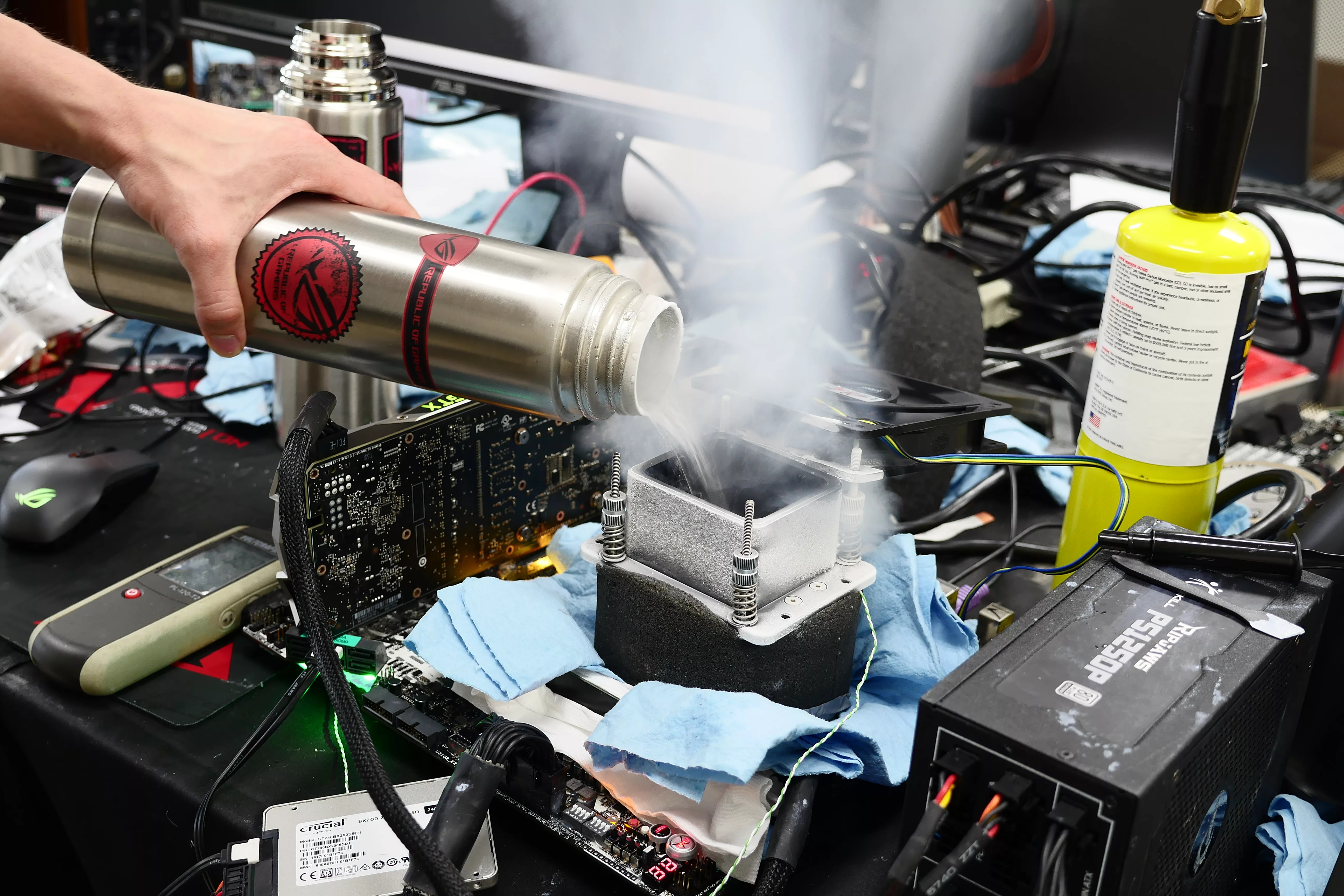
The Rampage VI Apex claims more performance victories with Intel's new Core i9-7940X and i9-7980XE
After dominating extreme overclocking with the first wave of Skylake-X CPUs, we've taken the latest 14- and 18-core models to sub-zero extremes.